
System
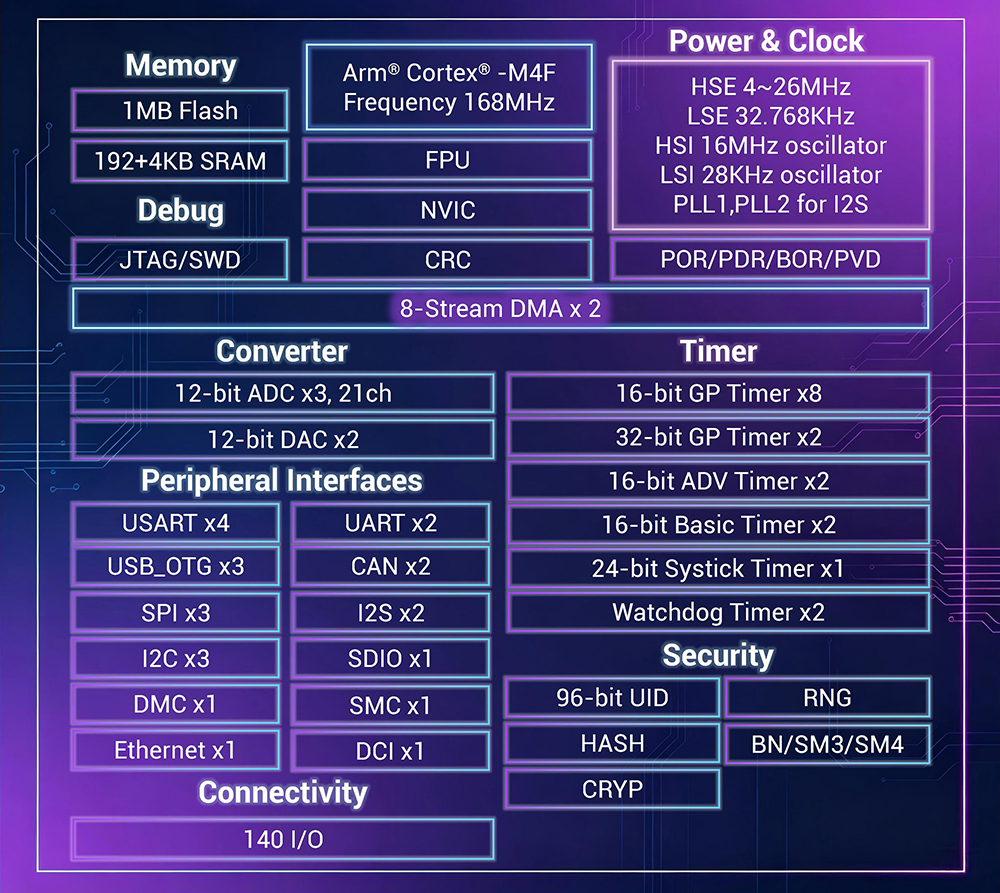
- Arm® Cortex® -M4F
- Working frequency up to 168MHz
- Support single FPU
- Support DSP instruction
Memory
- Flash: 1MB
- SRAM: 192KB+4KB
- Support external memory extension
Power Consumption
- VDD/VDDA: 1.8V~3.6V
- Backup domain power VBAT: 1.65~3.6V
- Support POR/PDR/BOR
- Support PVD
Timer
- 16/32-bit Universal Timer: 8/2
- 16-bit Advanced Timer: 2
- 16-bit Basic Timer: 2
- Watchdog Timer: 2
- 24-bit System Timer: 1
Analog Peripherals
- 12-bit ADC: 3, External channel: 24
- 12-bit DAC: 2
Security
- Support TRNG
- AES/DES/TDES
- BN/SM2/SM3/SM4
Debug Mode
- JTAG
- SWD
I/Os
- Up to 140 I/Os
- All I/Os are mappable on external interrupt vectors
Peripherals
- U(S)ART : 4+2
- I2C :3
- SPI : 3
- I2S : 2
- DCI : 1
- USB OTG : 3
- CAN: 2
- SDIO: 1
- Ethernet: 1
- EMMC : 1
- Support SDRAM
Package
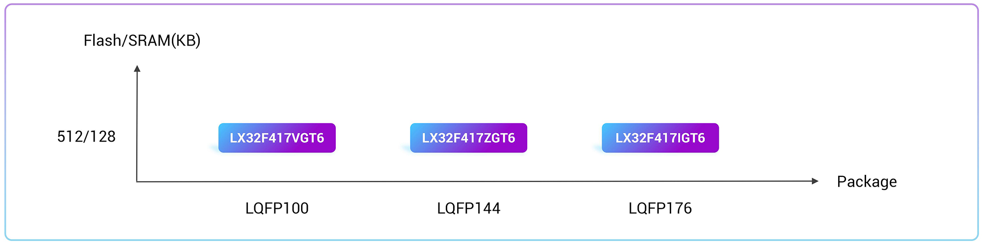
- LQFP100/144/176